
Applications
Electronics
ELECTRONICS
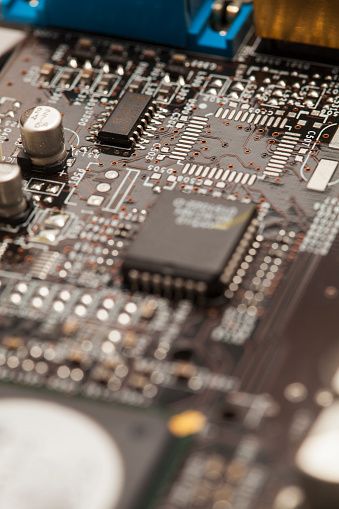
With the rapid scaling-down of chip size in microelectronics, the famous Moore’s law seems to reach the limit. In addition, the old paradigm for chip fabrication appears to become extremely economically challenging. In this regard, Atomic Layer Deposition (ALD) appears to be a very promising technique for highly scaled semiconductor devices fabrication in future microelectronics, especially for those extreme three-dimensional structures where thin films should be deposited conformally over the whole structures with atomic scale uniformity in thickness, composition and electrical chemical properties. ALD technology has already been largely used to for the fabrication of applications including memory and logic devices. In the process, ALD are mainly involved for the deposition of dielectric layer, sacrificial layers, electrode layers and barrier/seed layers. The common deposited materials are listed below.
Example:
 Dielectric layer: ZrO2/Al2O3/TiO2/HfO2/SrTiO3
Electrode layer: Ru/RuO2/TiN/ITO/Pt
Sacrificial: SiO2
Barrier/Seed layer: Ru
Cheol Seong Hwang, Chapter 8 Atomic Layer Deposition for Microelectronic Applications, Atomic Layer Deposition of Nanostructured Materials,Wiley, 2010
Nanotubular Electrostatic Capacitors for Electrical Energy Storage, Parag Banerjee, Israel Perez, Laurent Henn-Lecordier, Sang Bok Lee, and Gary W. Rubloff, Nature Nanotechnology 2009, 4, 292-296
Low temperature atomic layer deposition of high-k dielectric stacks for scaled metal-oxide-semiconductor devices, Ole Bethge, Stephan Abermann, Christoph Henkel, Emmerich Bertagnolli, Thin Solid Films 2009, 517, 5543–5547